What will computer chips look like in 2045?
Intel's leadership walks through how advanced process nodes are brought to volume, from yield learning and the lessons of 10nm to the shift from planar transistors to gate-all-around, High-NA EUV, backside power, and CFET. The discussion widens to the chip-to-chip bottleneck that hybrid bonding targets, the supply limits on EUV tooling as AI compute demand grows, and the economics that make foundry scale decisive.
Bringing a new process node to volume
Intel’s 14A has been in development for roughly three years, and the remaining work is about finalizing the tool set and fine-tuning each of the roughly 2,000 process steps so the line can run thousands of wafers a week, repeatably. Yield improvement runs on a continuous loop. Inline metrology flags defects as wafers move through the flow, end-of-line electrical test and sort reveal failures, and cross-sectioning in the TEM lab shows which layer a defect sits between, which points back to the section of the flow where it originated.
The central lesson from 10nm is that a node should carry only as much innovation as the schedule allows. 10nm was targeted for 2016 and did not reach manufacturing until 2018. Its hyperscaling ambitions forced process innovations to be invented without ready tools, which burdened both the process and the engineers. The technology that should have been deferred was EUV, which was not ready when 10nm was defined. TSMC moved EUV into volume manufacturing in 2019 and had about four more years of experience with the machines by the time Intel’s first EUV products shipped in 2023. Maturity is now gated through phase gates with yield, defect, and performance criteria. Technologies that miss a gate move on to a later node.
From planar to gate-all-around
Staying on schedule is hard partly because transistor designs take decades to mature. The planar MOS transistor from 1960 gave way to the FinFET, which wraps the gate around three sides of a silicon fin. Gate-all-around goes further by slicing the channel into nanoribbons that the gate surrounds completely. Building these ribbons requires alternating sacrificial placeholder layers that are etched away after hot steps near 1,000 degrees Celsius, followed by a high-k dielectric and then the gate metal. FinFET was demonstrated in 1989 and reached Intel volume production in 2011. Gate-all-around was demonstrated in 1988 but reached production at Samsung only in 2022.
The gap reflects how innovation was sequenced. Strained silicon, high-k metal gate, and FinFETs each delivered performance first, and gate-all-around became the next obvious step once those were exhausted. Each step also required tool vendors to invent new equipment, gases, and heating chucks. Chris Auth describes the R&D era shift clearly. In the 1980s and 1990s, Dennard scaling and lithography drove a predictable cadence of simply making things smaller. From the 2000s onward, the playbook opened up. Material counts have grown roughly tenfold since the 1990s, and atomic layer deposition now controls films atom by atom. The old instruction was to avoid changing anything, and the new one is to tear things up and try new ideas.
High-NA EUV and the economics of patterning
EUV prints at 13.5 nm, and High-NA raises the numerical aperture from 0.33 to 0.55. That lets it print features about 1.7 times smaller in a single pass. Without High-NA, the tightest patterns need two, three, or even four passes, and each extra pass consumes scarce tool time and adds defect risk. A High-NA scanner costs roughly twice as much as a standard EUV tool, so the decision turns on how many passes it eliminates.
Intel and TSMC reach different conclusions from the same tool because of architecture. Intel’s backside power relieves front-side pitch requirements, so High-NA can print the layers directly. TSMC lacks backside power, so it needs tighter front-side pitches and resorts to double-patterning with standard EUV. For Intel, High-NA is valuable. At 14A it is an option that is being negotiated customer by customer, because the value proposition comes with added complexity.
Backside power and the PDK
Power lines must be thick, while signal lines must be thin and widely spaced. In conventional designs, both have to be packed on top of the transistors. Backside power moves the power delivery to the back of the wafer, which frees room on top so signal lines can relax. Intel has spent decades as an integrated device manufacturer sharing transistor data internally, so a formal process design kit, the rulebook defining what a process can build, is new territory. The 18A PDK began without one and was refined through customer feedback. Maturity levels such as PDK 0.5, 0.9, and 1.0 now track quality, and 14A is expected to launch with a high-quality PDK from the outset.
Single-customer manufacturing has historically been a structural disadvantage. TSMC’s serving many customers gave it more wafers to learn from, more revenue to reinvest, and more pressure to hit deadlines. Enterprise-style requirements for foundry relationships are similarly demanding in their own right, from quality expectations to documentation.
Rethinking the chip stack
If the tech tree had diverged early, gate-all-around and backside power might never have become the path. Chris Auth argues that gate-all-around was close to inevitable as the ideal transistor, but that backside power and removing the substrate entirely are far more speculative. Copper will remain the workhorse for larger lines. For the tightest pitches, though, it will eventually be replaced. Ruthenium can be etched, so it avoids the liner that copper needs. That gives it an advantage at roughly 20 nm pitch, where the liner consumes a meaningful share of the conduction path. The choice of interconnect material is not fixed, since cobalt was once the leading option before copper returned to contention.
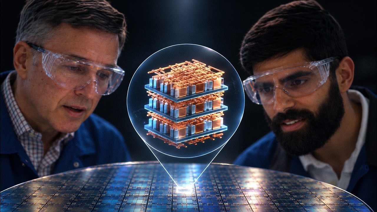
The bigger shift is vertical. Stacked transistors, or CFETs, pack n-type and p-type devices on top of one another and in principle double transistor density in the same area. The obstacles are cost, process complexity, and heat with no clear escape path. Power, frequency, and thermals are the three limits on compute, and thermal design for 3D devices is still in its infancy. Auth points to NAND and DRAM as proof that vertical structures are possible, and he suggests that a 20-year horizon makes exotic 3D logic plausible even though a four-year visibility window is what engineers can plan around today.
CFET is still in the lab. Intel and its competitors are evaluating it, and short-loop vehicles are used to resolve problems fast, testing simplified structures such as one nanoribbon stacked on one rather than four on four. The hardest parts are etching deep, high-aspect-ratio holes and filling them without leaving voids. Materials such as 2D transition-metal dichalcogenides can be deposited at atomic thickness, but a material is often eliminated for something as basic as poor adhesion or insufficient hermeticity that lets later steps change its properties.
Hot Topics and the cost of urgency
With thousands of open problems and limited wafers and engineering time, deciding where effort goes is one of the hardest parts of bringing up a node. Kevin Fischer, who runs the Hot Topics meetings, describes them as the point where risk is traded against the bottom line. The fundamental truth is that a complete dataset never arrives, so waiting for one means being too late. Epitaxial nodules are a concrete example. Abnormal, tumor-like epi growth can short a source or drain to the wrong neighbor and break transistors. Engineers work on several candidate fixes in parallel, since the obvious one is often not the one that works. Once a problem is classified as primary, resources are aligned into focused teams. A tiered hot-lot system then moves priority wafers through the factory, with the top tier taking precedence at every tool at the cost of efficiency across the whole line, much like a carpool lane.
Chip-to-chip bottlenecks and hybrid bonding
AI performance is often limited by how fast chips can exchange data rather than by raw computation. Doubling a chip’s width and length quadruples its area but only doubles its edge length, so as transistor density rises, computing grows faster than the ability to move data off the chip. Packaging evolved from side-by-side chips to silicon interposers, the so-called 2.5D approach, and then to direct bonding. Solder bumps add bulk and resistance, so hybrid bonding fuses copper interconnects directly by aligning, pressing, and heating the chips. The insulating surfaces bond at the same time. Intel’s Foveros is in volume production at about a 25 micrometer pitch and is moving below 10 micrometers. A published result has demonstrated a 0.45 micrometer pitch, and once pitches approach the sub-micron interconnect layers of the back end, bonding could connect lower layers across chips and reduce IR drop.
Wafer-to-wafer bonding dominates CMOS image sensors but requires matching dies, which makes yield harder to guarantee. Chip-to-wafer bonding lets known-good dies be tested and placed only on known-good bases, which makes it the natural choice for logic-to-logic stacking. Outside AI, hybrid bonding can cut interconnect power in picojoules per bit, which lowers both power and heat across interfaces such as CPU-to-GPU links.
Supply limits and the economics of scale
AI demand has been compounding at roughly 3x per year for a decade, while the EUV supply is constrained, with ASML producing fewer than 100 scanners a year and not planning to exceed that much by the end of the decade. Every fab, including TSMC’s and Intel’s, competes for the same tools, and memory makers such as SK Hynix are ramping as well. Once a process is locked to a specific tool, there is no substitute. CTO Pushkar Ranade estimates that Intel could roughly double leading-edge wafer output with today’s installed tool base, but not reach 10x, and that the constraint is industry-wide, because it requires the equipment supply chain and its suppliers to expand. Migrating from 18A to 14A should reuse roughly 80% of the tool set, but denser geometry requires new tools.
Fab economics are unusually dependent on scale. Around 80% of a fab’s cost is fixed, so each additional point of utilization or yield adds disproportionate revenue. Die yield moving from 60% to 70% is far more than a linear gain. Costs have also been doubling every four to five years, and a High-NA EUV scanner with associated equipment costs around $400 million. Consolidation has reduced the number of advanced-node foundries to three. The result is a shift from a vertically integrated industry toward a horizontal one, and now a pseudo-vertical one, as hyperscalers design their own chips and large AI labs could fill an entire fab on their own.
Catching up to TSMC
Intel’s gap with TSMC is primarily one of scale, not technology, according to Intel’s leadership. Within a few percent on performance, power, or density is not decisive. What matters is being on time and achieving high yields to support large, rapid ramps. Transistor density comparisons depend on multiple transistor flavors, SRAM variants, and analog and RF circuits, so a single metric is misleading. CapEx also matters. TSMC is expected to spend around $50 billion this year against Intel’s roughly $20 billion, although that comparison is unfair in part because Intel is still primarily building for itself while TSMC serves nearly everyone.
Terafab and rethinking the fab
Elon Musk’s Terafab effort reflects the same logic that drives the shortage. Companies needing large amounts of silicon may prefer guaranteed supply through their own fabs, though the bottleneck at the tool level means total silicon output will not rise simply because a new fab appears. Fabs also consume enormous power, water, and consumables, and those can be scaled more readily than tools. Raw cleanroom capacity is a further requirement.
Looking past current constraints, the risk-averse culture of semiconductor manufacturing is itself a barrier. Engineers are trained to treat the process flow as gospel, and incumbents will not gamble tens of billions on unproven changes. Auth and Ranade both argue that architecture, lithography passes, and even clean-room requirements are open questions. Transistor evolution from planar to FinFET to gate-all-around will continue, and chip design approaches locked in decades ago may deserve the same scrutiny.
The closing argument is about urgency. Ranade says that with hindsight, Intel should have invested more aggressively a year earlier, and that it will now invest more. The risk is that the US could be positioned to make trillions of dollars in advanced chips while the tools that make them remain concentrated elsewhere.